Thin Film Microstructure and Photo-physics
Through a combination of in-house spectroscopy techniques, alongside a complimentary assortment of synchrotron X-ray-based methods, members decipher the inherent microstructure of advanced thin film technologies at different length-scales, i.e. from several atoms to hundreds of unit cells. Through the effective merger of these approaches, this Research Theme aims to resolve the atomistic secrets of structurally complex and disordered optoelectronic materials and devices.
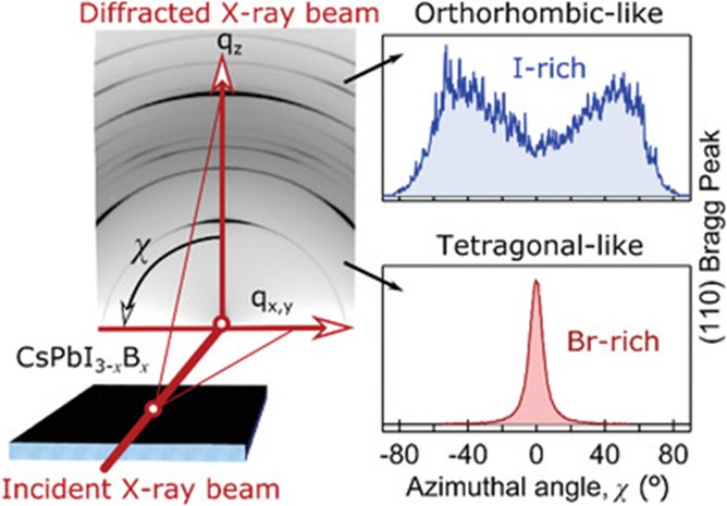
Figure 1 Polycrystalline CsPbI3−xBrx perovskite exhibits pervasive texture expressions (well-defined directions and distributions of grains) when solution processed into thin-film optical devices. Synchrotron-based large-area X-ray scattering techniques provide insights, which connect the final texture formation to the crystal composition and symmetry, defining the energetically favoured texture directions. Taken from Adv. Mater. 2007224 (2021).
References:
- Advanced Materials 2025, 2418300.
- Advanced Materials 2024,
- Advanced Energy Materials 2023,
- Advanced Materials 2021, 2007224.
- Science 2019, 365, 679.
Julian A. Steele
ARC DECRA Fellow
The University of Queensland, Australia
Jean Charles Ribierre
Asso. Professor
University of St Andrews, UK
Dechan Angmo
Senior Research Scientist
CSIRO, Australia
Toshinori Matsushima
Asso. Professor
Kyushu University, Japan
Jung Hwa Seo
Professor
University of Seoul, South Korea
Ebinazar Namdas
Asso. Professor
The University of Queensland, Australia
Shih-Chun Lo (Lawrence)
Asso. Professor
The University of Queensland, Australia